Balbharti Maharashtra State Board 11th Physics Important Questions Chapter 14 Semiconductors Important Questions and Answers.
Maharashtra State Board 11th Physics Important Questions Chapter 14 Semiconductors
Question 1.
What are the factors on which the electrical conductivity of any solid depends?
Answer:
Electrical conduction in a solid depends on its temperature, the number of charge carriers, how easily these carries can move inside a solid (mobility), its crystal structure, types, and the nature of defects present in a solid.
Question 2.
Why are metals good conductors of electricity?
Answer:
Metals are good conductors of electricity due to a large number of free electrons (≈ 1028 per m³) present in them.
![]()
Question 3.
Give the formula for the electrical conductivity of a solid and give the significance of the terms involved.
Answer:
The electrical conductivity (σ) of a solid is given by a = nqµ,
where n = charge carrier density (number of charge carriers per unit volume)
q = charge on the carriers
µ = mobility of carriers
Question 4.
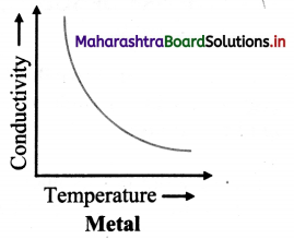
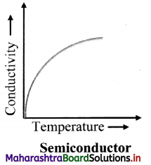
Explain in brief temperature dependence of electrical conductivity of metals and semiconductors with the help of graph.
Answer:
i. The electrical conductivity of a metal decreases with increase in its temperature.
ii. When the temperature of a semiconductor is increased, its electrical conductivity also increases
Question 5.
Mention the broad classification of semiconductors along with examples.
Answer:
A broad classification of semiconductors can be:
- Elemental semiconductors: Silicon, germanium
- Compound Semiconductors: Cadmium sulphide, zinc sulphide, etc.
- Organic Semiconductors: Anthracene, doped pthalocyanines, polyaniline etc.
Question 6.
What are some electrical properties of semiconductors?
Answer:
- Electrical properties of semiconductors are different from metals and insulators due to their unique conduction mechanism.
- The electronic configuration of the elemental semiconductors plays a very important role in their electrical properties.
- They are from the fourth group of elements in the periodic table.
- They have a valence of four.
- Their atoms are bonded by covalent bonds. At absolute zero temperature, all the covalent bonds are completely satisfied in a single crystal of pure semiconductor like silicon or germanium.
Question 7.
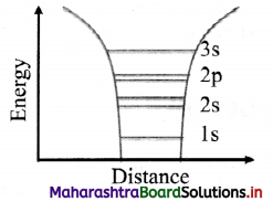
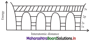
Explain in detail the distribution of electron energy levels in an isolated atom with the help of an example.
Answer:
- An isolated atom has its nucleus at the centre which is surrounded by a number of revolving electrons. These electrons are arranged in different and discrete energy levels.
- Consider the electronic configuration of sodium (atomic number 11) i.e, 1s², 2s², 2p6, 3s1. The outermost level 3s can take one more electron but it is half filled in sodium,
- The energy levels in each atom are filled according to Pauli’s exclusion principle which states that no two similar spin electrons can occupy the same energy level.
- That means any energy level can accommodate only two electrons (one with spin up state and the other with spin down state)
- Thus, there can be two states per energy level.
- Figure given below shows the allowed energy levels of a sodium atom by horizontal lines. The curved lines represent the potential energy of an electron near the nucleus due to Coulomb interaction.
Question 8.
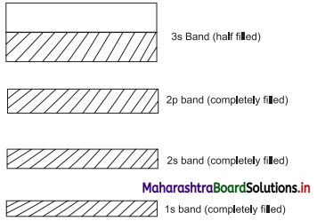
Explain formation of energy bands in solid sodium with neat labelled energy band diagrams.
Answer:
i. For an isolated sodium atom (atomic number 11) the electronic configuration is given as 1s², 2s², 2p6, 3s1. The outermost level 3s is half filled in sodium.
ii. The energy levels are filled according to Pauli’s exclusion principle.
iii. Consider two sodium atoms close enough so that outer 3s electrons can be considered equally to be part of any atom.
iv. The 3s electrons from both the sodium atoms need to be accommodated in the same level.
v. This is made possible by splitting the 3 s level into two sub-levels so that the Pauli’s exclusion principle is not violated. Figure given below shows the splitting of the 3 s level into two sub levels.
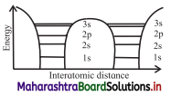
vi. When solid sodium is formed, the atoms come close to each other such that distance between them remains of the order of 2 – 3 Å. Therefore, the electrons from different atoms interact with each other and also with the neighbouring atomic cores.
vii. The interaction between the outer most electrons is more due to overlap while the inner most electrons remain mostly unaffected. Each of these energy levels is split into a large number of sub levels, of the order of Avogadro’s number due to number of atoms in solid sodium is of the order of this number.
viii. The separation between the sublevels is so small that the energy levels appear almost continuous. This continuum of energy levels is called an energy band. The bands are called 1 s band, 2s band, 2p band and so on. Figure shows these bands in sodium metal.
Question 9.
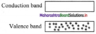
Explain concept of valence band and conduction band in solid crystal.
Answer:
A. Valence band (V.B):
- The topmost occupied energy level in an atom is the valence level. The energy band formed by valence energy levels of atoms in a solid is called the valence band.
- In metallic conductors, the valence electrons are loosely attached to the nucleus. At ordinary room temperature, some valence electrons become free. They do not leave the metal surface but can move from atom to atom randomly.
- Such free electrons are responsible for electric current through conductors.
B. Conduction band (C.B):
- The immediately next energy level that electrons from valence band can occupy is called conduction level. The band formed by conduction levels is called conduction band.
- It is the next permitted energy band beyond valence band.
- In conduction band, electrons move freely and conduct electric current through the solids.
- An insulator has empty conduction band.
Question 10.
Draw neat labelled diagram showing energy bands in sodium. Why broadening of higher bands is different than that of the lower energy bands?
Answer:
Broadening of valence and higher bands is more since interaction of these electrons is stronger than the inner most electrons.
Question 11.
State the conditions when electrons of a semiconductor can take part in conduction.
Answer:
- All the energy levels in a band, including the topmost band, in a semiconductor are completely occupied at absolute zero.
- At some finite temperature T, few electrons gain thermal energy of the order of kT, where k is the Boltzmann constant.
- Electrons in the bands between the valence band cannot move to higher band since these are already occupied.
- Only electrons from the valence band can be excited to the empty conduction band, if the thermal energy gained by these electrons is greater than the band gap.
- Electrons can also gain energy when an external electric field is applied to a solid. Energy gained due to electric field is smaller, hence only electrons at the topmost energy level gain such energy and participate in electrical conduction.
![]()
Question 12.
Define 1 eV.
Answer:
1 eV is the energy gained by an electron while it overcomes a potential difference of one volt. 1 eV= 1.6 × 10⁻¹⁹ J.
Question 13.
C, Si and Ge have same lattice structure. Why is C insulator while Si and Ge intrinsic semiconductors?
Answer:
- The 4 valence electrons of C, Si or Ge lie respectively in the second, third and fourth orbit.
- Energy required to take out an electron from these atoms (i.e., ionisation energy Eg) will be least for Ge, followed by Si and highest for C.
- Hence, number of free electrons for conduction in Ge and Si are significant but negligibly small for
Question 14.
What is intrinsic semiconductor?
Answer:
A pure semiconductor is blown as intrinsic semiconductor.
Question 15.
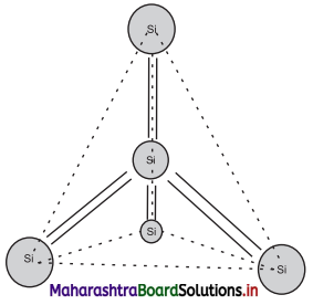
Explain characteristics and structure of silicon using a neat labelled diagram.
Answer:
- Silicon (Si) has atomic number 14 and its electronic configuration is 1s² 2s² 2p6 3s² 3p².
- Its valence is 4.
- Each atom of Si forms four covalent bonds with its neighbouring atoms. One Si atom is surrounded by four Si atoms at the comers of a regular tetrahedron as shown in the figure.
Question 16.
Describe in detail formation of holes in ii. intrinsic semiconductor.
Answer:
i. In intrinsic semiconductor at absolute zero temperature, all valence electrons are tightly bound to respective atoms and the covalent bonds are complete.
ii. Electrons are not available to conduct electricity through the crystal because they cannot gain enough energy to get into higher energy levels.
iii. At room temperature, however, a few covalent bonds are broken due to heat energy produced by random motion of atoms. Some of the valence electrons can be moved to the conduction band. This creates a vacancy in the valence band as shown in figure.
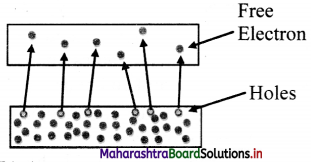
iv. These vacancies of electrons in the valence band are called holes. The holes are thus absence of electrons in the valence band and they carry an effective positive charge.
Question 17.
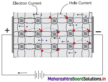
How does electric conduction take place inside a pure silicon?
Answer:
- There are two different types of charge carriers in a pure semiconductor. One is the electron and the other is the hole or absence of electron.
- Electrical conduction takes place by transportation of both carriers or any one of the two carriers in a semiconductor.
- When a semiconductor is connected in a circuit, electrons, being negatively charged, move towards positive terminal of the battery.
- Holes have an effective positive charge, and move towards negative terminal of the battery. Thus, the current through a semiconductor is carried by two types of charge carriers moving in opposite directions.
- Figure given below represents the current through a pure silicon.
Question 18.
Why do holes not exist in conductor?
Answer:
- In case of semiconductors, there is one missing electron from one of the covalent bonds.
- The absence of electron leaves an empty space called as hole; each hole carries an effective positive charge.
- In case of an conductor, number of free electrons are always available for conduction. There is no absence of electron in it. Hence holes do not exist in conductor.
Question 19.
What is the need for doping an intrinsic semiconductor?
Answer:
The electric conductivity of an intrinsic semiconductor is very low at room temperature; hence no electronic devices can be fabricated using them. Addition of a small amount of a suitable impurity to an intrinsic semiconductor increases its conductivity appreciably. Hence, intrinsic semiconductors are doped with impurities.
Question 20.
Explain what is doping.
Answer:
- The process of adding impurities to an intrinsic semiconductor is called doping.
- The impurity atoms are called dopants which may be either trivalent or pentavalent. The parent atoms are called hosts.
- The dopant material is so selected that it does not disturb the crystal structure of the host.
- The size and the electronic configuration of the dopant should be compatible with that of the host.
- Doping is expressed in ppm (parts per million), i.e., one impurity atom per one million atoms of the host.
- Doping significantly increases the concentration of charge carriers.
Question 21.
What is extrinsic semiconductors?
Answer:
The semiconductor with impurity is called a doped semiconductor or an extrinsic semiconductor.
Question 22.
Draw neat diagrams showing schematic electronic structure of:
i. A pentavalent atom [Antimony (Sb)]
ii. A trivalent atom [Boron (B)]
Answer:
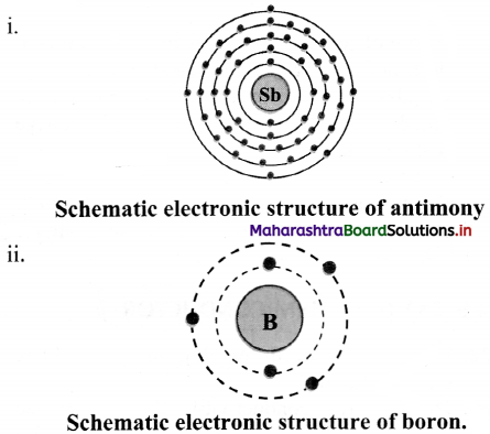
[Note: Electronic structure of antimony is drawn as per its electronic configuration in accordance with Modern Periodic Table.]
Question 23.
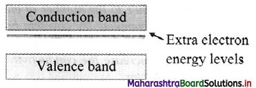
With the help of neat diagram, explain the structure of n-type semiconductor in detail.
Answer:
i. When silicon or germanium crystal is doped with a pentavalent impurity such as phosphorus, arsenic, or antimony we get n-type semiconductor.
ii. When a dopant atom of 5 valence electrons occupies the position of a Si atom in the crystal lattice, 4 electrons from the dopant form bonds with 4 neighbouring Si atoms and the fifth electron from the dopant remains very weakly bound to its parent atom
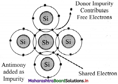
iii. To make this electron free even at room temperature, very small energy is required. It is 0.01 eV for Ge and 0.05 eV for Si.
iv. As this semiconductor has large number of electrons in conduction band and its conductivity is due to negatively charged carriers, it is called n-type semiconductor.
v. The n-type semiconductor also has a few electrons and holes produced due to the thermally broken bonds.
vi. The density of conduction electrons (ne) in a doped semiconductor is the sum total of the electrons contributed by donors and the thermally generated electrons from the host.
vii. The density of holes (nh) is only due to the thermally generated holes of the host Si atoms.
viii. Thus, the number of free electrons exceeds the number of holes (ne >> nh). Thus, in n-type semiconductor electrons are the majority carriers and holes are the minority carriers.
![]()
Question 24.
What are some features of n-type semiconductor?
Answer:
- These are materials doped with pentavalent impurity (donors) atoms.
- Electrical conduction in these materials is due to majority charge carriers i.e., electrons.
- The donor atom loses electrons and becomes positively charged ions.
- Number of free electrons is very large compared to the number of holes, ne >> nh. Electrons are majority charge carriers.
- When energy is supplied externally, negatively charged free electrons (majority charges carries) and positively charged holes (minority charges carries) are available for conduction.
Question 25.
With the help of neat diagram, explain the structure of p-type semiconductor in detail.
Answer:
i. When silicon or germanium crystal is doped with a trivalent impurity such as boron, aluminium or indium, we get a p-type semiconductor.
ii. The dopant trivalent atom has one valence electron less than that of a silicon atom. Every trivalent dopant atom shares its three electrons with three neighbouring Si atoms to form covalent bonds. But the fourth bond between silicon atom and its neighbour is not complete.
iii. The incomplete bond can be completed by another electron in the neighbourhood from Si atom.
iv. The shared electron creates a vacancy in its place. This vacancy or the absence of electron is a hole.
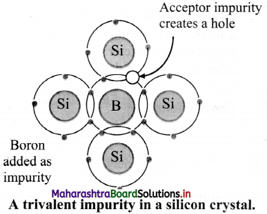
v. Thus, a hole is available for conduction from each acceptor impurity atom.
vi. Holes are majority carriers and electrons are minority carriers in such materials. Acceptor atoms are negatively charged ions and majority carriers are holes. Therefore, extrinsic semiconductor doped with trivalent impurity is called a p-type semiconductor.
vii. For a p-type semiconductor, nh >> ne.
Question 26.
What are some features of p-type semiconductors?
Answer:
- These are materials doped with trivalent impurity atoms (acceptors).
- Electrical conduction in these materials is due to majority charge carriers i.e., holes.
- The acceptor atoms acquire electron and become negatively charged-ions.
- Number of holes is very large compared to the number of free electrons. nh >> ne. Holes are majority charge carriers.
- When energy is supplied externally, positively charged holes (majority charge carriers) and negatively charged free electrons (minority charge carriers) are available for conduction.
Question 27.
What are donor and acceptor impurities?
Answer:
- Every pentavalent dopant atom which donates one electron for conduction is called a donor impurity.
- Each trivalent atom which can accept an electron is called an acceptor impurity.
Question 28.
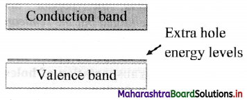
Explain the energy levels of both donor and acceptor impurities with a schematic band structure.
Answer:
i. The free electrons donated by the donor impurity atoms occupy energy levels which are in the band gap and are close to the conduction band.
ii. The vacancies of electrons or the extra holes are created in the valence band due to addition of acceptor impurities. The impurity levels are created just above the valence band in the band gap.
Question 29.
Distinguish between p-type and n-type semiconductor.
Answer:
| p-type semiconductor | n-type semiconductor |
| 1. The impurity of some trivalent element like B, Al, In, etc. is mixed with semiconductor. | The impurity of some pentavalent element like P, As, Sb, etc. is mixed |
| 2. The impurity atom accepts one electron hence the impurities | The impurity atom donates – one electron, hence the impurities added are known as donor impurities. |
| 3. The holes are majority charge carriers and electrons are minority charge carriers. | The electrons are j majority charge carriers and holes are minority charge carriers. |
| 4. The acceptor energy level is close to the valence band and far away from conduction band. | Donor energy level is close to the conduction band and far away from valence band. |
Question 30.
What is the charge on a p-type and n-type semiconductor?
Answer:
n-type as well as p-type semiconductors are electrically neutral.
Question 31.
Explain the transportation of holes inside a p-type semiconductor.
Answer:
i. Consider a p-type semiconductor connected to terminals of a battery as shown.
ii. When the circuit is switched on, electrons at 1 and 2 are attracted to the positive terminal of the battery and occupy nearby holes at x and y. This creates holes at the positions 1 and 2 previously occupied by electrons.
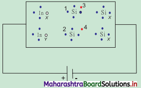
iii. Next, electrons at 3 and 4 move towards the positive terminal and create holes in their previous positions.
iv. But, the holes are captured at the negative terminal by the electrons supplied by the battery.
v. In this way, holes are transported from one place to other and density of holes is kept constant so long as the battery is working.
Question 32.
A pure Si crystal has 4 × 1028 atoms m-3. It is doped by 1 ppm concentration of antimony. Calculate the number of electrons and holes. Given n1 = 1.2 × 10¹⁶/m³.
Answer:
As, the atom is doped with 1 ppm concentration of antimony (Sb).
1 ppm = 1 parts per one million atoms. = 1/106
∴ no. of Si atoms = \(\frac {Total no. of Si atoms}{10^6}\)
= \(\frac {4×10^{28}}{10^6}\) = 4 × 10²² m-3
i.e., total no. of extra free electrons (ne)
= 4 × 10²² m-3
ni2 = ne nh
∴ nh = \(\frac {n_i^2}{n_e}\) = \(\frac {(1.2×10^{16})^2}{4×10^{22}}\)
= \(\frac {144×10^{30}{4×10^{22}}\)
= 36 × 10-8
= 3.6 × 10⁹ m-3.
Question 33.
A pure silicon crystal at temperature of 300 K has electron and hole concentration 1.5 × 10¹⁶ m-3 each. (ne = nh). Doping bv indium increases nh to 4.5 × 10²² m-3. Calculate ne for the doped silicon crystal.
Answer:
Given: At 300 K, ni = ne = nh = 1.5 × 10¹⁶ m-3
After doping nh = 4.5 × 10²² m-3
To find: Number density of electrons (ne)
Formula: ni² = ne nnh
Calculation From formula:
ne = \(\frac {n_i^2}{n_h}\) = \(\frac {(1.5×10^{16})^2}{4×10^{22}}\)
= \(\frac {255×10^{30}{45×10^{21}}\)
= 5 × 10⁻⁹ m-3.
![]()
Question 34.
A Ge specimen is doped with A/. The concentration of acceptor atoms is ~1021 atoms/m³. Given that the intrinsic concentration of electron-hole pairs is ~10 19/m³, calculate the concentration of electrons in the specimen.
Answer:
Given: At room temperature,
ni = ne = nh = 1019 m-3
After doping nh = 1021 m-3
To find: Number density of electrons (nc)
Formulae: ni2 = nenh
Calculation: From formula,
ne = \(\frac {n_i^2}{n_h}\) = \(\frac {(10^{19})^2}{10^{21}}\)
= \(\frac {255×10^{30}{45×10^{21}}\)
= 1017 m-3.
Question 35.
A semiconductor has equal electron and hole concentration of 2 × 10⁸ m-3. On doping with a certain impurity, the electron concentration increases to 4 × 10¹⁰ m-3, then calculate the new hole concentration of the semiconductor.
Answer:
Given: ni = 2 × 10⁸ m-3, n = 4 × 10¹⁰ m-3
After doping nh = 1021 m-3
To find: Number density of holes (nh)
Formulae: ni 2= nenh
Calculation: From formula.
nh = \(\frac {n_i^2}{n_e}\) = \(\frac {(2×10^{8})^2}{4×10^{10}}\) = 106 m-3
Question 36.
What is a p-n junction?
Answer:
When n-type and p-type semiconductor materials are fused together, the junction formed is called as p-n junction.
Question 37.
Explain the process of diffusion in p-n junction.
Answer:
i. The transfer of electrons and holes across the p-n junction is called diffusion.
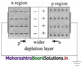
ii. When an n-type and a p-type semiconductor materials are fused together, initially, the number of electrons in the n-side of a junction is very large compared to the number of electrons on the p-side. The same is true for the number of holes on the p-side and on the n-side.
iii. Thus, a large difference in density of carriers exists on both sides of the p-n junction. This difference causes migration of electrons from the n-side to the p-side of the
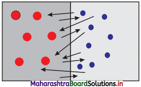
iv. They fill up the holes in the p-type material and produce negative ions.
v. When the electrons from the n-side of a junction migrate to the p-side, they leave behind positively charged donor ions on the n- side. Effectively, holes from the p-side migrate into the n-region.
vi. As a result, in the p-type region near the junction there are negatively charged acceptor ions, and in the n-type region near the junction there are positively charged donor ions.
vii. The extent up to which the electrons and the holes can diffuse across the junction depends on the density of the donor and the acceptor ions on the n-side and the p-side respectively, of the junction.
Question 38.
Define potential barrier.
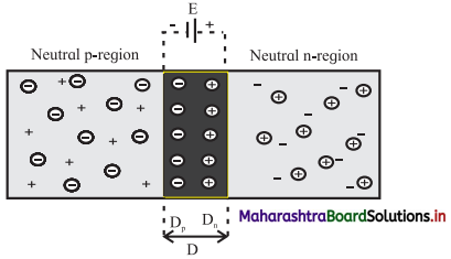
Answer:
The diffusion of carriers across the junction and resultant accumulation of positive and negative charges across the junction builds a potential difference across the junction. This potential difference is called the potential barrier.
Question 39.
Draw neat labelled diagrams for potentials barrier and depletion layer in a p-n junction.
Answer:
Question 40.
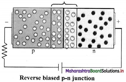
Explain in brief electric field across a p-n junction with a neat labelled diagram.
Answer:
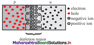
- When p-type semiconductor is fused with n-type semiconductor, a depletion region is developed across the junction.
- The n-side near the boundary of a p-n junction becomes positive with respect to the p-side because it has lost electrons and the p-side has lost holes.
- Thus, the presence of impurity ions on both sides of the junction establishes an electric field across this region such that the n-side is at a positive voltage relative to the p-side.
Question 41.
What is the need of biasing a p-n junction?
Answer:
- Due to potential barrier across depletion region, charge carriers require extra energy to overcome the barrier.
- A suitable voltage needs to be applied to the junction externally, so that these charge carriers can overcome the potential barrier and move across the junction.
Question 41.
Explain the mechanism of forward biased p-n junction.
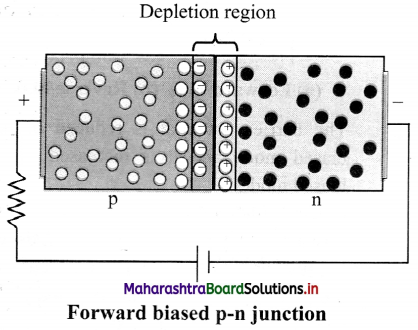
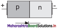
Answer:
- In forward bias, a p-n junction is connected in an electric circuit such that the p-region is connected to the positive terminal and the n-region is connected to the negative terminal of an external voltage source.
- The external voltage effectively opposes the built-in potential of the junction. The width of potential barrier is thus reduced.
- Also, negative charge carriers (electrons) from the n-region are pushed towards the junction.
- A similar effect is experienced by positive charge carriers (holes) in the p-region and they are pushed towards the junction.
- Both the charge carriers thus find it easy to cross over the barrier and contribute towards the electric current.
Question 42.
Explain the mechanism of reverse biased p-n junction.
Answer:
i. In reverse biased, the p-region is connected to the negative terminal and the n-region is connected to the positive terminal of the external voltage source. This external voltage effectively adds to the built-in potential of the junction. The width of potential barrier is thus increased.
ii. Also, the negative charge carriers (electrons) from the n-region are pulled away from the junction.
iii. Similar effect is experienced by the positive charge carriers (holes) in the p-region and they are pulled away from the junction.
iv. Both the charge carriers thus find it very difficult to cross over the barrier and thus do not contribute towards the electric current.
Question 43.
State some important features of the depletion region.
Answer:
- It is formed by diffusion of electrons from n-region to the p-region. This leaves positively charged ions in the n-region.
- The p-region accumulates electrons (negative charges) and the n-region accumulates the holes (positive charges).
- The accumulation of charges on either sides of the junction results in forming a potential barrier and prevents flow of charges.
- There are no charges in this region.
- The depletion region has higher potential on the n-side and lower potential on the p-side of the junction.
![]()
Question 44.
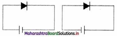
What is p-n junction diode? Draw its circuit symbol.
Answer:
A p-n junction, when provided with metallic connectors on each side is called a junction diode
Question 45.
Explain asymmetrical flow of current in p-n junction diode in detail.
Answer:
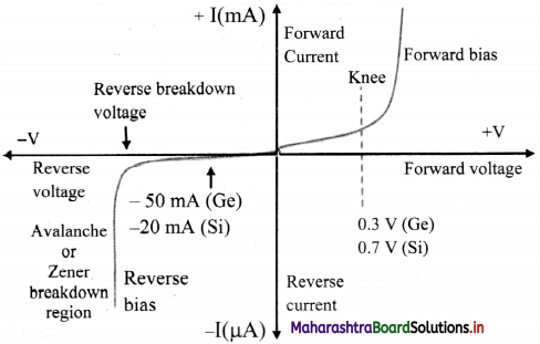
i. The barrier potential is reduced in forward biased mode and it is increased in reverse biased mode.
ii. Carriers find it easy to cross the junction in forward bias and contribute towards current because the barrier width is reduced and they are pushed towards the junction and gain extra energy to cross the junction.
iii. The current through the diode in forward bias is large and of the order of a few milliamperes (10-3 A) for a typical diode.
iv. When connected in reverse bias, width of the potential barrier is increased and the carriers are pushed away from the junction so that very few carriers can cross the junction and contribute towards current.
v. This results in a very small current through a reverse biased diode. The current in reverse biased diode is of the order of a few microamperes (10-6 A).
vi. When the polarity of bias voltage is reversed, the width of the depletion layer changes. This results in asymmetrical current flow through a diode as shown in figure.
Question 46.
What is knee voltage?
Answer:
In forward bias mode, the voltage for which the current in a p-n junction diode rises sharply is called knee voltage.
Question 47.
What is a forward current in case of zero biased p-n junction diode?
Answer:
When the diode terminals are shorted together, some holes (majority carriers) in the p-side have enough thermal energy to overcome the potential barrier. Such carriers cross the barrier potential and contribute to current. This current is known as the forward current.
Question 48.
Define reverse current in zero biased p-n junction diode.
Answer:
When the diode terminals are shorted together some holes generated in the n-side (minority carriers), move across the junction and contribute to current. This current is known as the reverse current.
Question 49.
Explain the I-V characteristics of a reverse biased junction diode.
Answer:
i. The positive terminal of the external voltage is connected to the cathode (n-side) and negative terminal to the anode (p-side) across the diode.
ii. In case of reverse bias the width of the depletion region increases and the p-n junction behaves like a high resistance.
iii. Practically no current flows through it with an increase in the reverse bias voltage. However, a very small leakage current does flow through the junction which is of the order of a few micro amperes, (µA).
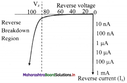
iv. When the reverse bias voltage applied to a diode is increased to sufficiently large value, it causes the p-n junction to overheat. The overheating of the junction results in a sudden rise in the current through the junction. This is because covalent bonds break and a large number of carries are available for conduction. The diode thus no longer behaves like a diode. This effect is called the avalanche breakdown.
v. The reverse biased characteristic of a diode is shown in figure.
Question 50.
Explain zero biased junction diode.
Answer:
i. When a diode is connected in a zero bias condition, no external potential energy is applied to the p-n junction.
li. The potential barrier that exists in a junction prevents the diffusion of any more majority carriers across it. However, some minority carriers (few free electrons in the p-region and few holes in the n-region) drift across the junction.
iii. An equilibrium is established when the majority carriers are equal in number (ne = nh) and both moving in opposite directions. The net current flowing across the junction is zero. This is a state of‘dynamic equilibrium’.
iv. The minority carriers are continuously generated due to thermal energy.
v. When the temperature of the p-n junction is raised, this state of equilibrium is changed.
vi. This results in generating more minority carriers and an increase in the leakage current. An electric current, however, cannot flow through the diode because it is not connected in any electric circuit
Question 51.
What is dynamic equilibrium?
Answer:
An equilibrium is established when the majority carriers are equal in number (ne = nh) and both moving in opposite directions. The net current flowing across the junction is zero. This is a state of‘dynamic equilibrium’.
Question 52.
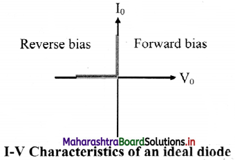
Draw a neat diagram and state I-V characteristics of an ideal diode.
Answer:
An ideal diode offers zero resistance in forward biased mode and infinite resistance in reverse biased mode.
Question 53.
What do you mean by static resistance of a diode?
Answer:
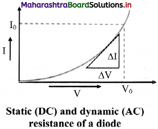
Static (DC) resistance:
- When a p-n junction diode is forward biased, it offers a definite resistance in the circuit. This resistance is called the static or DC resistance (Rg) of a diode.
- The DC resistance of a diode is the ratio of the DC voltage across the diode to the DC current flowing through it at a particular voltage.
- It is given by, Rg = \(\frac {V}{I}\)
Question 54.
Explain dynamic resistance of a diode.
Answer:
- The dynamic (AC) resistance of a diode, rg, at a particular applied voltage, is defined as
rg = \(\frac {∆V}{∆I}\) - The dynamic resistance of a diode depends on the operating voltage.
- It is the reciprocal of the slope of the characteristics at that point.
Question 55.
Draw a graph representing static and dynamic resistances of a diode.
Answer:
Question 56.
Refer to the figure as shown below and find the resistance between point A and B when an ideal diode is (i) forward biased and (ii) reverse biased.
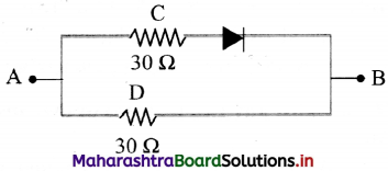
Answer:
We know that for an ideal diode, the resistance is zero when forward biased and infinite when reverse biased.
i. Figure (a) shows the circuit when the diode is forward biased. An ideal diode behaves as a conductor and the circuit is similar to two resistances in parallel.
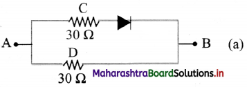
∴ RAB = (30 × 30)/(30 +30) = 900/60 = 15 Ω
ii. Figure (b) shows the circuit when the diode is reverse biased.
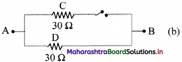
It does not conduct and behaves as an open switch along path ACB. Therefore, RAB = 30 Ω. the only resistance in the circuit along the path ADB.
![]()
Question 57.
State advantages of semiconductor devices.
Answer:
- Electronic properties of semiconductors can be controlled to suit our requirement.
- They are smaller in size and light weight.
- They can operate at smaller voltages (of the order of few mV) and require less current (of the order of pA or mA), therefore, consume lesser power.
- Almost no heating effects occur, therefore these devices are thermally stable.
- Faster speed of operation due to smaller size.
- Fabrication of ICs is possible.
Question 58.
State disadvantages of semiconductor devices.
Answer:
- They are sensitive to electrostatic charges.
- Not very useful for controlling high power.
- They are sensitive to radiation.
- They are sensitive to fluctuations in temperature.
- They need controlled conditions for their manufacturing.
- Very few materials are semiconductors.
Question 59.
Explain applications of semiconductors.
Answer:
i. Solar cell:
- It converts light energy into electric energy.
- t is useful to produce electricity in remote areas and also for providing electricity for satellites, space probes and space stations.
ii. Photo resistor: It changes its resistance when light is incident on it.
iii. Bi-polar junction transistor:
- These are devices with two junctions and three terminals.
- A transistor can be a p-n-p or n-p-n transistor.
- Conduction takes place with holes and electrons.
- Many other types of transistors are designed and fabricated to suit specific requirements.
- They are used in almost all semiconductor devices.
iv. Photodiode: It conducts when illuminated with light.
v. LED (Light Emitting Diode):
- It emits light when current passes through it.
- House hold LED lamps use similar technology.
- They consume less power, are smaller in size and have a longer life and are cost effective.
vi. Solid State Laser: It is a special type of LED. It emits light of specific frequency. It is smaller in size and consumes less power.
vii. Integrated Circuits (ICs): A small device having hundreds of diodes and transistors performs the work of a large number of electronic circuits.
Question 60.
Explain any four application of p-n junction diode.
Answer:
1. Solar cell:
- It converts light energy into electric energy.
- It is useful to produce electricity in remote areas and also for providing electricity for satellites, space probes and space stations.
ii. Photodiode: It conducts when illuminated with light.
iii. LED (Light Emitting Diode):
- It emits light when current passes through it.
- House hold LED lamps use similar technology.
- They consume less power, are smaller in size and have a longer life and are cost effective.
iv. Solid State Laser: It is a special type of LED. It emits light of specific frequency. It is smaller in size and consumes less power.
Question 61.
What is thermistor?
Answer:
Thermistor is a temperature sensitive resistor. Its resistance changes with change in its temperature.
Question 62.
What are different ty pes of thermistor and what are their applications?
Answer:
There are two types of thermistor:
i. NTC (Negative Thermal Coefficient) thermistor: Resistance of a NTC thermistor decreases with increase in its temperature. Its temperature coefficient is negative. They are commonly used as temperature sensors and also in temperature control circuits.
ii. PTC (Positive Thermal Coefficient) thermistor: Resistance of a PTC thermistor increases with increase in its temperature. They are commonly used in series with a circuit. They are generally used as a reusable fuse to limit current passing through a circuit to protect against over current conditions, as resettable fuses.
Question 63.
How are thermistors fabricated?
Answer:
Thermistors are made from thermally sensitive metal oxide semiconductors. Thermistors are very sensitive to changes in temperature.
![]()
Question 64.
Enlist any two features of thermistor.
Answer:
- A small change in surrounding temperature causes a large change in their resistance.
- They can measure temperature variations of a small area due to their small size.
Question 65.
Write a note on:
i. Electric devices
ii. Electronic devices
Answer:
i. Electric devices:
- These devices convert electrical energy into some other form.
- Examples: Fan, refrigerator, geyser etc. Fan converts electrical energy into mechanical energy. A geyser converts it into heat energy.
- They use good conductors (mostly metals) for conduction of electricity.
- Common working range of currents for electric circuits is milliampere (mA) to ampere.
- Their energy consumption is also moderate to high. A typical geyser consumes about 2.0 to 2.50 kW of power.
- They are moderate to large in size and are costly.
ii. Electronic devices:
- Electronic circuits work with control or sequential changes in current through a cell.
- A calculator, a cell phone, a smart watch or the remote control of a TV set are some of the electronic devices.
- Semiconductors are used to fabricate such devices.
- Common working range of currents for electronic circuits it is nano-ampere to µA.
- They consume very low energy. They are very compact, and cost effective.
Question 66.
Can we take one slab of p-type semiconductor and physically join it to another n-type semiconductor to get p-n junction?
Answer:
- No. Any slab, howsoever flat, will have roughness much larger than the inter-atomic crystal spacing (~2 to 3 Å).
- Hence, continuous contact at the atomic level will not be possible. The junction will behave as a discontinuity for the flowing charge carriers.
Question 67.
What is Avalanche breakdown and zener breakdown?
Answer:
i. Avalanche breakdown: In high reverse bias, minority carriers acquire sufficient kinetic energy and collide with a valence electron. Due to collisions the covalent bond breaks. The valence electron enters conduction band. A breakdown occurring in such a manner is avalanche breakdown. It occurs with lightly doped p-n junctions.
ii. Zener breakdown: It occurs in specially designed and highly doped p-n junctions, viz., zener diodes. In this case, covalent bonds break directly due to application of high electric field. Avalanche breakdown voltage is higher than zener voltage.
Question 68.
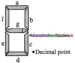
Indicators on platform, digital clocks, calculators make use of seven LEDs to indicate a number. How do you think these LEDs might be arranged?
Answer:
i. The indicators on platforms, digital clocks, calculators are made using seven LEDs arranged in such a way that when provided proper signal they light up displaying desired alphabet or number.
ii. This arrangement of LEDs is called Seven Segment Display.
Multiple Choice Questions
Question 1.
The number of electrons in the valence shell of semiconductor is ……………
(A) less than 4
(B) equal to 4
(C) more than 4
(D) zero
Answer:
(B) equal to 4
Question 2.
If the temperature of semiconductor is increased, the number of electrons in the valence band will ……………….
(A) decrease
(B) remains same
(C) increase
(D) either increase or decrease
Answer:
(A) decrease
Question 3.
When N-type semiconductor is heated, the ……………..
(A) number of electrons and holes remains same.
(B) number of electrons increases while that of holes decreases.
(C) number of electrons decreases while that of holes increases.
(D) number of electrons and holes increases equally.
Answer:
(D) number of electrons and holes increases equally.
Question 4.
In conduction band of solid, there is no electron at room temperature. The solid is ……………
(A) semiconductors
(B) insulator
(C) conductor
(D) metal
Answer:
(B) insulator
![]()
Question 5.
In the crystal of pure Ge or Si, each covalent bond consists of …………..
(A) 1 electron
(B) 2 electrons
(C) 3 electrons
(D) 4 electrons
Answer:
(B) 2 electrons
Question 6.
A pure semiconductor is ……………..
(A) an extrinsic semiconductor
(B) an intrinsic semiconductor
(C) p-type semiconductor
(D) n-type semiconductor
Answer:
(B) an intrinsic semiconductor
Question 7.
For an extrinsic semiconductor, the valency of the donor impurity is …………..
(A) 2
(B) 1
(C) 4
(D) 5
Answer:
(D) 5
Question 8.
In a semiconductor, acceptor impurity is
(A) antimony
(B) indium
(C) phosphorous
(D) arsenic
Answer:
(B) indium
Question 9.
What are majority carriers in a semiconductor?
(A) Holes in n-type and electrons in p-type.
(B) Holes in n-type and p-type both.
(C) Electrons in n-type and p-type both.
(D) Holes in p-type and electrons in n-type.
Answer:
(D) Holes in p-type and electrons in n-type.
Question 10.
When a hole is produced in P-type semiconductor, there is ……………….
(A) extra electron in valence band.
(B) extra electron in conduction band.
(C) missing electron in valence band.
(D) missing electron in conduction band.
Answer:
(C) missing electron in valence band.
Question 11.
The number of bonds formed in p-type and n-type semiconductors are respectively
(A) 4,5
(B) 3,4
(C) 4,3
(D) 5,4
Answer:
(B) 3,4
Question 12.
The movement of a hole is brought about by the valency being filled by a ………………..
(A) free electrons
(B) valence electrons
(C) positive ions
(D) negative ions
Answer:
(B) valence electrons
Question 13.
The drift current in a p-n junction is
(A) from the p region to n region.
(B) from the n region to p region.
(C) from n to p region if the junction is forward biased and from p to n region if the junction is reverse biased.
(D) from p to n region if the junction is forward biased and from n to p region if the junction is reverse biased.
Answer:
(B) from the n region to p region.
Question 14.
If a p-n junction diode is not connected to any circuit, then
(A) the potential is same everywhere.
(B) potential is not same and n-type side has lower potential than p-type side.
(C) there is an electric field at junction direction from p-type side to n-type side.
(D) there is an electric field at the junction directed from n-type side to p-type side.
Answer:
(D) there is an electric field at the junction directed from n-type side to p-type side.
Question 15.
In an unbiased p-n junction, holes diffuse from the p-region to n-region because
(A) free electrons in the n-region attract them.
(B) they move across the junction by the potential difference.
(C) hole concentration in p-region is more as compared to n-region.
(D) all the above.
Answer:
(C) hole concentration in p-region is more as compared to n-region.
Question 16.
The width of depletion region ……………
(A) becomes small in forward bias of diode
(B) becomes large in forward bias of diode
(C) is not affected upon by the bias
(D) becomes small in reverse bias of diode
Answer:
(A) becomes small in forward bias of diode
Question 17.
For p-n junction in reverse bias, which of the following is true?
(A) There is no current through P-N junction due to majority carriers from both regions.
(B) Width of potential barriers is small and it offers low resistance.
(C) Current is due to majority carriers.
(D) Both (B) and (C)
Answer:
(A) There is no current through P-N junction due to majority carriers from both regions.
![]()
Question 18.
In the circuit shown below Di and D2 are two silicon diodes. The current in the circuit is …………….
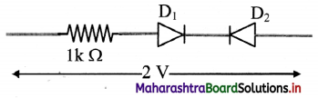
(A) 2 A
(B) 2 mA
(C) 0.8 mA
(D) very small (approx 0)
Answer:
(D) very small (approx 0)
Question 19.
For an ideal junction diode,
(A) forward bias resistance is infinity.
(B) forward bias resistance is zero.
(C) reverse bias resistance is infinity.
(D) both (B) and (C).
Answer:
(D) both (B) and (C).